|
Advanced structural materials and coupled properties
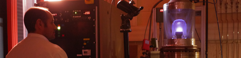
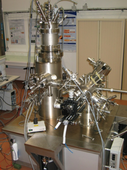
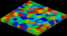
Finely architectured materials for structural or/and functional applications: based on the existence of high level platforms concerning the elaboration, the transformation, the characterization of various materials, coupled with some expertise in multiscale modelling,
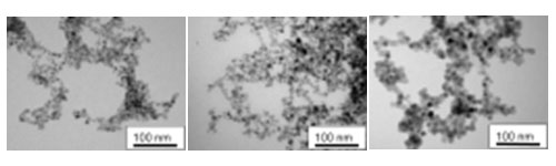
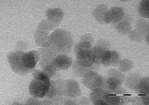
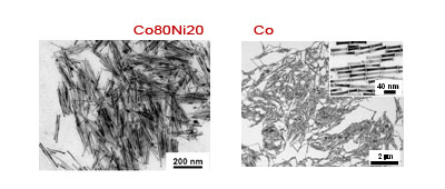
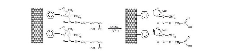
it becomes naturally consistent to develop even more widely the design of new multifunctional materials and their validation through modeling; some examples already exist within the LABEX such as the elaboration of ultrahard materials (LSPM), permanent magnets from Co nanowires (ITODYS and MSC), hybrid materials composed of soft components (foams, sprays, polymers) and inorganics components (nanoparticles, polyometallic or alkooxydes, ...) (MSC), multiferroic materials (LSPM), ..... In this field, only the imagination of the researchers can limit the extent of their work; up to now, the efforts are mainly put on the elaboration and modeling steps. By adding some contributions on the characterization side, the LABEX will become more and more convincing in the development of industrial collaborations.
Functionalized structural materials.
For all these structural materials which are asked to become " smarter ", and to resist to more and
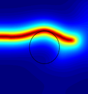
more severe environments, it becomes also essential investigating their coupled properties as well as the interaction between a given material and it environment. In the field of multi-scale modelling, some coupled properties (mechanical and thermal, magnetic, electrical,....) have already been successfully predicted in LSPM for a wide variety of materials. Some teams in MSC work on the development of porous materials that present a good capacity of reducing the vibrations or the sounds and that can be incorporated into structural materials for constructions or aeronautic applications. Also, the investigation of the behaviour of materials under severe
|